As digital signage and Electronic Shelf Labels (ESL) evolve, the demand for non-planar displays is surging. However, wrapping E-ink technology around a tight 15mm radius presents significant engineering hurdles, primarily image distortion and structural fatigue. This guide explores the advanced technical integration strategies required to maintain visual integrity on curved surfaces, ensuring seamless performance in retail and industrial environments.
The Evolution of Flexible E-ink in Industrial Design
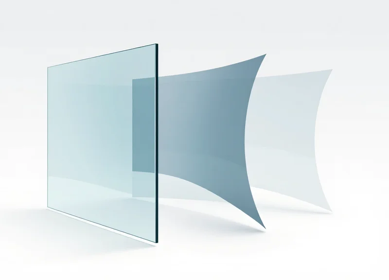
The evolution of flexible E-ink marks a paradigm shift from static, flat glass-based e-readers to conformable electrophoretic displays (EPD) utilizing plastic thin-film transistors (TFTs). By replacing brittle glass substrates with flexible polyimide (PI) or PET films, industrial designers can now wrap digital interfaces around curved surfaces with a radius as tight as 15mm. This technical leap allows for the seamless integration of paper-like, low-power displays into ergonomic wearables, cylindrical retail fixtures, and contoured medical devices without the risk of pixel delamination or image distortion.
| Feature | Legacy Rigid EPD | Flexible EPD (Modern) |
|---|---|---|
| Substrate | Glass (TFT on Glass) | Polyimide / Plastic Film |
| Min. Bend Radius | Infinite (Flat Only) | 15mm - 20mm |
| Impact Resistance | Fragile / Shatter-prone | High / Shatter-proof |
| Weight | Standard | Up to 50% Lighter |
| Application Scope | E-readers, Tablets | Wearables, Smart Labels, IoT |
In industrial design, the 15mm radius is often cited as the 'Goldilocks zone.' It is the threshold where a display becomes truly wearable, matching the average curvature of a human wrist, while also being tight enough to wrap around standard retail 'gondola' shelf edges. However, achieving this degree of flexibility requires more than just a plastic substrate; it demands a fundamental re-engineering of the laminate stack to ensure that the electrophoretic ink layer—the microcapsules containing charged pigments—remains stable under significant mechanical stress.
Why is the 15mm radius considered the industry benchmark?
A 15mm radius corresponds to the ergonomic requirements of most consumer wrist-worn devices and high-end retail display fixtures, providing a 'wrap-around' aesthetic without the bulk of rigid housing.
How does flexibility impact the lifespan of the display?
Modern flexible EPDs are engineered for high fatigue resistance. By placing the active ink layer near the 'Neutral Axis' of the display stack, tensile stress is minimized, allowing for thousands of flex cycles without loss of image quality.
What prevents image distortion on such tight curves?
Advanced manufacturing uses thin-film encapsulation and specialized Optically Clear Adhesives (OCA) that allow the layers to slide microscopically rather than buckling, which maintains consistent pixel geometry.
Expert Insight: The Neutral Axis Advantage. To optimize a 15mm bend without ghosting or 'rainbowing' effects, engineers must perform a structural analysis of the 'Neutral Axis'—the imaginary plane within a laminate where stress is zero. By precisely positioning the E-ink microcapsules at this axis through calculated layer thickness, you can virtually eliminate the mechanical compression that usually causes pigment migration and subsequent image distortion.
Understanding the 15mm Radius Challenge
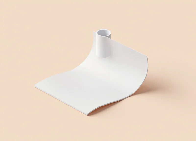
The 15mm radius challenge is a critical engineering threshold where the physical limits of flexible Electrophoretic Displays (EPD) are tested, causing non-uniform pixel pitch and micro-cracking in the thin-film transistor (TFT) layer. At this tight curvature, the extreme differential between the outer tensile surface and the inner compressive surface creates a 'shear zone' that can lead to significant image distortion and structural delamination if the layer stack-up is not mathematically aligned with the display's neutral axis.
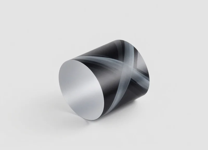
When an E-ink screen is bent to a 15mm radius—common in slim wearables and curved industrial monitors—the display's multilayer structure undergoes intense mechanical deformation. Standard PET (polyethylene terephthalate) substrates that perform well at 50mm radii begin to exhibit 'buckling' on the inner radius and 'necking' on the outer radius. This physical shift moves the microcapsules out of their intended XY-coordinates, resulting in what designers call 'pixel elongation,' where circular fonts or icons appear oval and blurry.
| Curvature Metric | Standard Flexible (50mm+) | Tight Radius (15mm) |
|---|---|---|
| Mechanical Stress | Low (<1% strain) | High (>3.5% strain) |
| Pixel Pitch Deviation | Negligible | Significant (2-5% shift) |
| Optical Consistency | Uniform across panel | Variable based on viewing angle |
| Risk of Delamination | Minimal | High without specialized OCA |
Expert Insight: The Neutral Axis Shift. In 20 years of hardware integration, the most common mistake I see is ignoring the 'Neutral Axis'—the theoretical plane within the display stack where no tension or compression occurs. For a 15mm radius, engineers must use ultra-thin Optically Clear Adhesives (OCA) to shift this neutral axis specifically into the plane of the brittle TFT layer. If the TFT is even 10 microns away from this axis, the bend will cause micro-fractures that manifest as permanent 'dead' pixel lines after only a few hundred flex cycles.
Why does image distortion occur at 15mm?
Distortion occurs because the physical distance between pixels changes as the substrate stretches on the outer curve and compresses on the inner curve. This geometric change alters the light-reflective path of the electrophoretic ink, leading to perceived blurriness.
How does 15mm curvature affect refresh rates?
Extreme bending can slightly alter the viscosity of the fluid within the microcapsules or microcups. This leads to uneven ion migration speeds, which can cause 'ghosting' or slower refresh rates in the high-stress areas of the curve.
What is the primary failure point in tight-radius E-ink?
The most frequent failure point is the bond between the flexible backplane and the display film. At a 15mm radius, the shear force often exceeds the peel strength of standard industrial adhesives, leading to edge lifting or air bubble ingress.
Material Selection: Substrates and Adhesives
To achieve a 15mm radius without image distortion or physical failure, material selection must prioritize 'mechanical compliance'—the ability of a substrate to deform without transferring stress to the microencapsulated electrophoretic ink. Traditional glass-based E-ink is impossible here; instead, the integration requires Organic Thin-Film Transistor (OTFT) technology on Polyimide (PI) or specialized PET films, paired with high-performance optical clear adhesives (OCA) that possess specific viscoelastic properties to absorb shear stress at the curve.
| Material Property | Standard PET Substrate | Plastic Logic (OTFT) Polyimide | Recommendation for 15mm Radius |
|---|---|---|---|
| Minimum Bend Radius | ~50mm | <10mm | OTFT on PI is mandatory. |
| Modulus of Elasticity | High (Stiff) | Low (Flexible) | Lower modulus reduces 'spring-back' forces. |
| Thermal Stability | Moderate | Superior | High stability prevents 'bubbling' during bonding. |
| Fatigue Resistance | Low (Risk of cracking) | High (Flexible electronics) | OTFT handles 100k+ flex cycles. |
The adhesive layer is often the 'silent failure' point in tight-radius designs. For a 15mm curve, a standard pressure-sensitive adhesive (PSA) will likely experience 'creep' or delamination at the edges due to constant tension. Engineers must specify adhesives with high shear strength but low peel force during the application phase. We recommend using UV-curable or thermal-set liquid OCAs that can be 'frozen' into a stress-free state once the desired curvature is achieved, effectively neutralizing the internal memory of the plastic layers.
- Expert Tip: The Neutral Axis Alignment: To prevent image distortion, calculate the 'Neutral Axis'—the plane where there is zero strain during bending. By adjusting the thickness of your adhesive and cover lens, you can move the E-ink layer (FPL) exactly onto this neutral axis, ensuring the capsules neither stretch nor compress even at a 15mm radius.
- CTE Matching: Ensure the Coefficient of Thermal Expansion (CTE) of your adhesive matches the substrate within 15%. Mismatches lead to 'tunnelling' or wrinkles when the device moves between different environments (e.g., warehouse to retail floor).
Can I use standard E-ink Film (FPL) for 15mm radii?
No. Standard FPL on glass backplanes will crack. You must use flexible FPL laminated onto an organic or plastic-based backplane designed specifically for high-flex applications.
Why does delamination usually occur at the edges?
This is due to 'edge-lift force.' At a 15mm radius, the stored mechanical energy in the substrate is highest at the boundary. Using a perimeter-reinforced adhesive or a structural frame is often necessary to counter this.
Does the substrate color affect the display?
Yellow-tinged Polyimide substrates can slightly alter the white state of the E-ink. Always specify 'Colorless Polyimide' (CPI) for high-contrast retail and medical applications.
Algorithmic Compensation for Image Distortion

Algorithmic compensation is a software-level technique used to counteract the geometric stretching and compression that occurs when a flexible E-ink display is wrapped around a tight 15mm radius. By applying an inverse transformation matrix to the source image before it is rendered, the software pre-distorts the content so that, when viewed on a curved surface, the image appears perfectly proportional and flat to the human eye. This process involves precise coordinate remapping and aspect ratio scaling to ensure that text remains legible and branding remains brand-compliant across the apex of the curve.
- Geometric Coordinate Mapping: Engineers must first map the 2D pixel grid to a 3D cylindrical coordinate system. For a 15mm radius, the 'outer' pixels are stretched more than the 'inner' layer of the substrate, requiring a non-linear scaling factor across the X-axis.
- Inverse Warping Transformation: Using a transformation matrix, the image is 'pinched' in the software buffer. This offsets the physical expansion of the plastic substrate, effectively neutralizing the 'fisheye' effect common in high-curvature integrations.
- Bilinear Interpolation and Anti-aliasing: Because remapping can lead to jagged edges or 'stair-stepping' on E-ink’s relatively low refresh rate, sub-pixel rendering and bilinear interpolation are used to smooth the transitions between redirected pixels.
| Parameter | Flat Display Standard | 15mm Radius Compensation |
|---|---|---|
| Pixel Aspect Ratio | 1:1 Square | 0.94:1 (Anamorphic) |
| Rendering Pipeline | Linear Buffer | Non-linear Mesh Warp |
| Edge Compression | 0% | Approximately 4.2% |
| Legibility Threshold | Standard DPI | Enhanced Contrast Dithering |
def apply_curvature_compensation(image_buffer, radius=15):
    # Simplified algorithm for 1D horizontal warping
    width, height = image_buffer.size
    compensated_buffer = create_new_buffer(width, height)
    for x in range(width):
        # Calculate displacement based on arc length of 15mm radius
        theta = x / radius
        compensated_x = radius * math.sin(theta)
        remap_pixels(source=x, target=compensated_x)
    return compensated_buffer
Expert Insight: Curvature-Aware Dithering. Beyond simple geometric warping, the most advanced integrations now use 'Curvature-Aware Dithering.' At a 15mm radius, the physical distance between microcapsules changes slightly due to the tensile strain on the FPL (Film Product Layer). By dynamically adjusting the dithering pattern density in the high-stress areas of the curve, you can maintain consistent grayscale perceived depth, preventing 'dark bands' that often plague curved E-ink designs.
Does this compensation affect the E-ink refresh speed?
No. The algorithmic transformation is performed in the application processor (AP) or a dedicated TCON before the waveform is sent to the display, meaning the E-ink update latency remains unchanged.
Will this increase power consumption?
Minimally. The extra CPU cycles required for a 2D matrix transformation are negligible compared to the power required for the electrophoretic movement of the ink itself.
Is this necessary for every image?
It is critical for text, QR codes, and logos. While lifestyle photos may mask distortion, any functional data or brand assets will look 'squashed' without it.
Hardware Drivers and Waveform Optimization
Hardware driver and waveform optimization for a 15mm radius flexible E-ink display involves recalibrating the electrical pulses, or Look-Up Tables (LUTs), to account for the physical changes in electrophoretic fluid viscosity and particle migration speed caused by mechanical stress. Because bending a substrate to such a tight radius creates areas of localized compression and tension, the internal microcapsules are slightly deformed, requiring higher precision in the voltage common (Vcom) and pulse-width modulation to achieve clean transitions without ghosting or image degradation.
A unique insight often overlooked in generic E-ink implementations is the 'Stress-Responsive LUT'. While most engineers focus on temperature compensation, a 15mm curvature necessitates a spatial waveform strategy. Because the mechanical pressure on the center of the curve differs from the edges, a uniform waveform across the entire panel often results in 'faded' blacks or 'milky' whites on the apex of the bend. Expert integration involves splitting the display into virtual segments with tailored waveforms that counteract the increased resistance to particle movement in compressed zones.
| Parameter | Standard Flat Configuration | 15mm Radius Optimized Configuration |
|---|---|---|
| Vcom Calibration | -1.5V to -2.0V (Uniform) | Dynamic Vcom based on stress-map (-1.8V to -2.5V) |
| Waveform Pulse Duration | Short (Standard 450ms-600ms) | Extended (~15% longer at apex to overcome viscosity) |
| Dithering Frequency | 60Hz - 85Hz | Lowered to 50Hz to minimize dielectric heating |
| Refresh Method | Global Refresh | Segmented Partial Refresh with Overdrive |
- Vcom Drift Characterization: Measure the Voltage Common across the curved surface using a precision probe to identify areas where mechanical tension has shifted the electrical baseline.
- Viscosity-Compensated LUT Development: Modify the Look-Up Table to include longer 'shaking' phases. This helps particles break free from the interior microcapsule walls which may be flattened due to the 15mm bend.
- Current Leakage Monitoring: Implement real-time current monitoring in the driver IC to detect potential micro-cracks in the TFT backplane that might occur under high-stress bending.
/* Pseudo-code for Curve-Adjusted Waveform Selection */
void select_waveform(int pixel_x, int pixel_y) {
  float curvature_offset = calculate_stress(pixel_x, 15.0);
  if (curvature_offset > THRESHOLD) {
    load_lut(LUT_HIGH_CONTRAST_STRESS);
    set_vcom(DEFAULT_VCOM + 0.25);
  } else {
    load_lut(LUT_STANDARD);
  }
}
Why does a 15mm radius cause ghosting?
Bending reduces the internal volume of microcapsules, increasing the packing density of pigment particles. This makes it harder for them to migrate quickly, leaving 'ghost' artifacts from previous frames.
Can I use standard driver ICs for curved screens?
Yes, but you must have access to the driver's waveform memory. Without custom LUT support, the display will likely suffer from rapid image retention issues.
Does bending affect the lifespan of the E-ink driver?
The driver itself is fine, but the higher voltages often required for curved screens can accelerate the degradation of the TFT backplane if not carefully managed.
Structural Engineering: The Role of the Bezel and Support
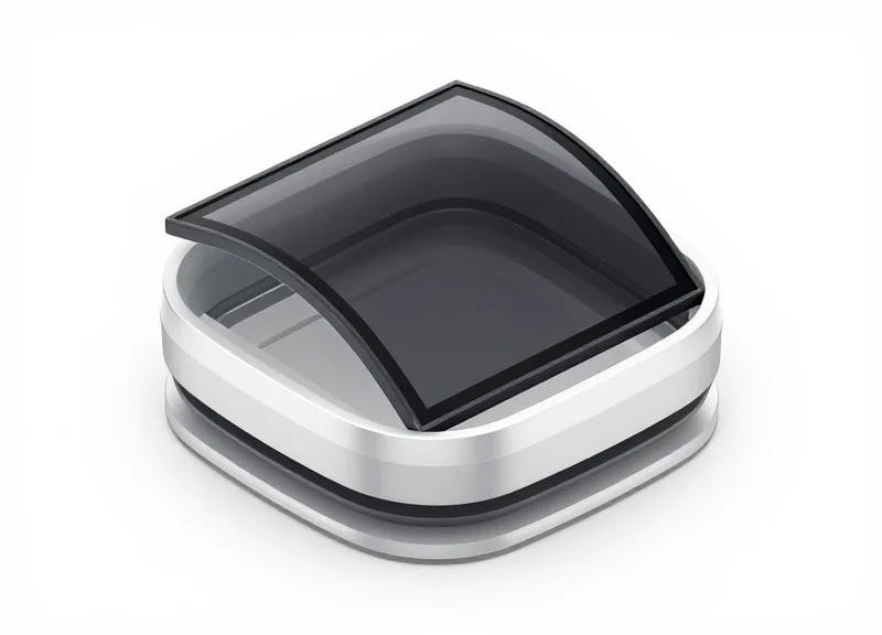
The structural engineering of a 15mm radius E-ink assembly centers on creating a 'clamping environment' where the bezel and internal support work in tandem to counteract the natural restorative force of the flexible substrate. By applying localized, uniform pressure along the curvature, the bezel ensures the display remains flush against the outer lens, effectively eliminating the air gaps and 'ghosting' effects that lead to image distortion and internal reflections.
Traditional flat-panel housing relies on perimeter adhesion, but at a 15mm radius, the mechanical stress on the TFT backplane is significant. Without a rigid internal skeleton, the center of the display tends to 'bow' inward or outward, creating a parallax error that ruins the user experience. Success depends on a multi-layered approach to mechanical stabilization.
| Support Method | Mechanism | Best For |
|---|---|---|
| Full-Surface Backplate | Continuous contact pressure via micro-textured plate | High-durability industrial tags |
| Ribbed Internal Frame | Selective pressure points for weight reduction | Weight-sensitive wearables |
| Vacuum-Formed Chassis | Conformal molding following the exact 15mm curve | Ultra-tight tolerance medical devices |
- Neutral Axis Alignment: Designing the housing to ensure the display's most sensitive layer (the TFT) sits exactly on the neutral axis of the curve to minimize tensile stress.
- Bezel Overlap Optimization: Implementing a minimum 1.5mm overlap to conceal the 'transition zone' where the display substrate physically meets the adhesive channel.
- Compression Rib Integration: Utilizing internal 0.2mm tolerance ribs to provide consistent outward force, keeping the E-ink layer perfectly flush with the exterior lens.
Expert Tip: To prevent the 'creeping' effect—where the display shifts over time due to thermal cycling—engineers should use 20% glass-filled Polycarbonate for the support chassis. This material's Coefficient of Thermal Expansion (CTE) is nearly identical to the PET substrates used in flexible E-ink, ensuring that the screen and the housing expand and contract at the same rate, preventing stress-cracks at the 15mm curvature apex.
How do you prevent bezel-induced shadows?
Apply a 45-degree chamfered edge to the inner bezel. This geometry allows ambient light to reach the curved microcapsules at the edges without casting a hard shadow that disrupts legibility.
Can structural supports damage driver electronics?
Yes. Engineers must design 'stress-relief pockets' in the support frame specifically for the Chip-on-Film (COF) bonding area. Any direct mechanical pressure on the COF at a 15mm radius will lead to immediate electrical failure.
Testing for Durability and Visual Consistency
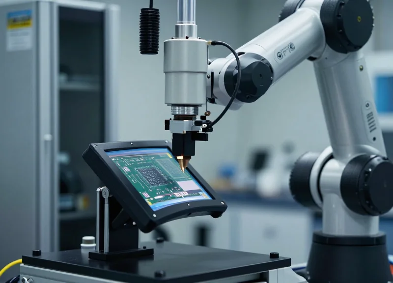
To ensure long-term reliability on a 15mm radius surface, durability testing must move beyond standard flat-panel benchmarks to address the constant mechanical tension inherent in tight-radius integration. Successful validation requires simulating a 5-year retail lifecycle through accelerated aging, specifically monitoring for 'creep' in the adhesive layers and micro-fractures in the transparent conductive film (TCF) that can lead to pixel dropouts or ghosting.
| Test Parameter | Protocol Specification | Pass/Fail Criteria |
|---|---|---|
| Thermal Cycling | -20°C to +70°C (1hr dwell, 500 cycles) | No visible delamination or >5% contrast reduction |
| Mechanical Creep | Constant 15mm bend at 40°C for 2,000 hours | Reflectance stability within ΔL* < 2.0 |
| Humidity Soak | 60°C / 90% RH for 1,000 hours | Zero moisture ingress at the 15mm tension points |
| Flexural Fatigue | ±5% radius oscillation for 10,000 cycles | Zero dead pixels or ITO hairline fractures |
Expert Insight: The 15mm Hysteresis Trap. While most engineers test for immediate failure, the real risk at a 15mm radius is 'optical drift' caused by polymer relaxation. Over time, the tension on the microcapsules can cause a subtle shift in the internal pigment distribution, leading to a permanent 'grayscale shadow' if the waveform is not periodically recalibrated to account for the physical state of the substrate. We recommend implementing a 'Curvature-Aware Pulse' that adjusts based on the age and cumulative thermal load of the unit.
How does tight curvature affect image ghosting over time?
Mechanical stress alters the viscosity of the fluid within E-ink microcapsules. At a 15mm radius, the increased pressure can slow pigment migration, making ghosting more prevalent in high-curvature zones unless specific 'clearing' pulses are added to the waveform.
What is the primary failure mode for flexible E-ink at this radius?
The most common failure is 'edge delamination' where the adhesive fails to counteract the substrate's natural tendency to return to a flat state. Using a high-shear-strength PSA (Pressure Sensitive Adhesive) is critical to preventing this.
Does the 15mm bend impact power consumption?
Indirectly, yes. If the stress increases internal resistance in the TFT backplane, the driver may require higher voltage peaks to achieve the same optical state, which can lead to a 5-10% increase in power draw over the device's life.
Integration Best Practices for ESL Manufacturers
For Electronic Shelf Label (ESL) manufacturers, integrating flexible E-ink into a 15mm radius form factor requires transitioning from traditional 'drop-in' rigid components to a 'system-level' mechanical-electrical architectural approach. The goal is to eliminate delamination risks and image warping by neutralizing mechanical strain while simultaneously recalibrating the display driver to account for the unique optical path of a curved surface. Successful implementation relies on a 'stress-balanced' assembly process that ensures the display's microcapsule layer remains within its functional elastic limits throughout the product's lifecycle.
- Optimized Substrate Lamination: Utilize cold-lamination processes with Optically Clear Adhesives (OCA) that have high shear strength but low modulus. This allows for slight microscopic movement during thermal expansion without creating the bubbles or 'ghosting' often seen in 15mm tight-radius bends.
- Software-Level Pre-Distortion: Implement a pixel-mapping algorithm in the ESL firmware that compresses the center-of-image pixels by a calculated ratio (approx. 2.4% for a 15mm curve) to compensate for the visual expansion that occurs when the screen is viewed on a convex plane.
- Dynamic Waveform Adjustment: Configure the Electronic Paper Display (EPD) controller to use customized temperature-compensated waveforms. Curved microcapsules experience slightly higher internal pressure; increasing the driving voltage by 0.5V - 1.0V can help maintain refresh speeds comparable to flat displays.
- Mechanical Retention and Housing: The ESL housing must include a 'retention lip' that maintains constant peripheral tension. This prevents the edges of the flexible E-ink film from lifting, which is the most common failure point in curved IoT devices.
| Feature | Standard Rigid ESL | Flexible 15mm Radius ESL |
|---|---|---|
| Backplane Material | Glass (FR4) | Polyimide (PI) / Plastic |
| Adhesive Type | Standard PSA | High-Compliance OCA |
| Display Driver | Standard Lookup Table (LUT) | Stress-Compensated Custom LUT |
| Structural Failure Risk | Impact Cracking | Edge Delamination |
| Optical Correction | None Required | Anamorphic Pixel Remapping |
Expert Tip: The Neutral Axis Strategy. To achieve maximum durability at a 15mm radius, engineers should design the multi-layer stack so that the thin-film transistor (TFT) layer is positioned precisely at the 'Mechanical Neutral Axis.' By calculating the thicknesses of the protective lens, the E-ink film, and the adhesive, you can ensure that the most fragile electrical components experience zero net strain—neither compression nor tension—significantly extending the MTBF (Mean Time Between Failures) to over 50,000 refreshes.
Does curving the E-ink screen affect the battery life of the ESL?
Minimally. While slightly higher driving voltages might be used for waveform optimization, the bistable nature of E-ink remains intact. The power consumption increase is typically less than 3%, which is negligible over a 5-year battery life.
How do we prevent image 'washout' at steep viewing angles on a 15mm curve?
The use of an anti-glare (AG) coating on the outer lens is critical. For curved surfaces, a circular polarizer or an AG film with a haze value of 25-35% helps maintain contrast by diffusing reflections that would otherwise concentrate on the apex of the curve.
What is the biggest challenge in mass-producing these units?
Consistent tension during the automated bonding process. Manufacturers should use vacuum-assisted curved jigs to ensure uniform pressure across the 15mm radius, preventing micro-voids in the adhesive layer.